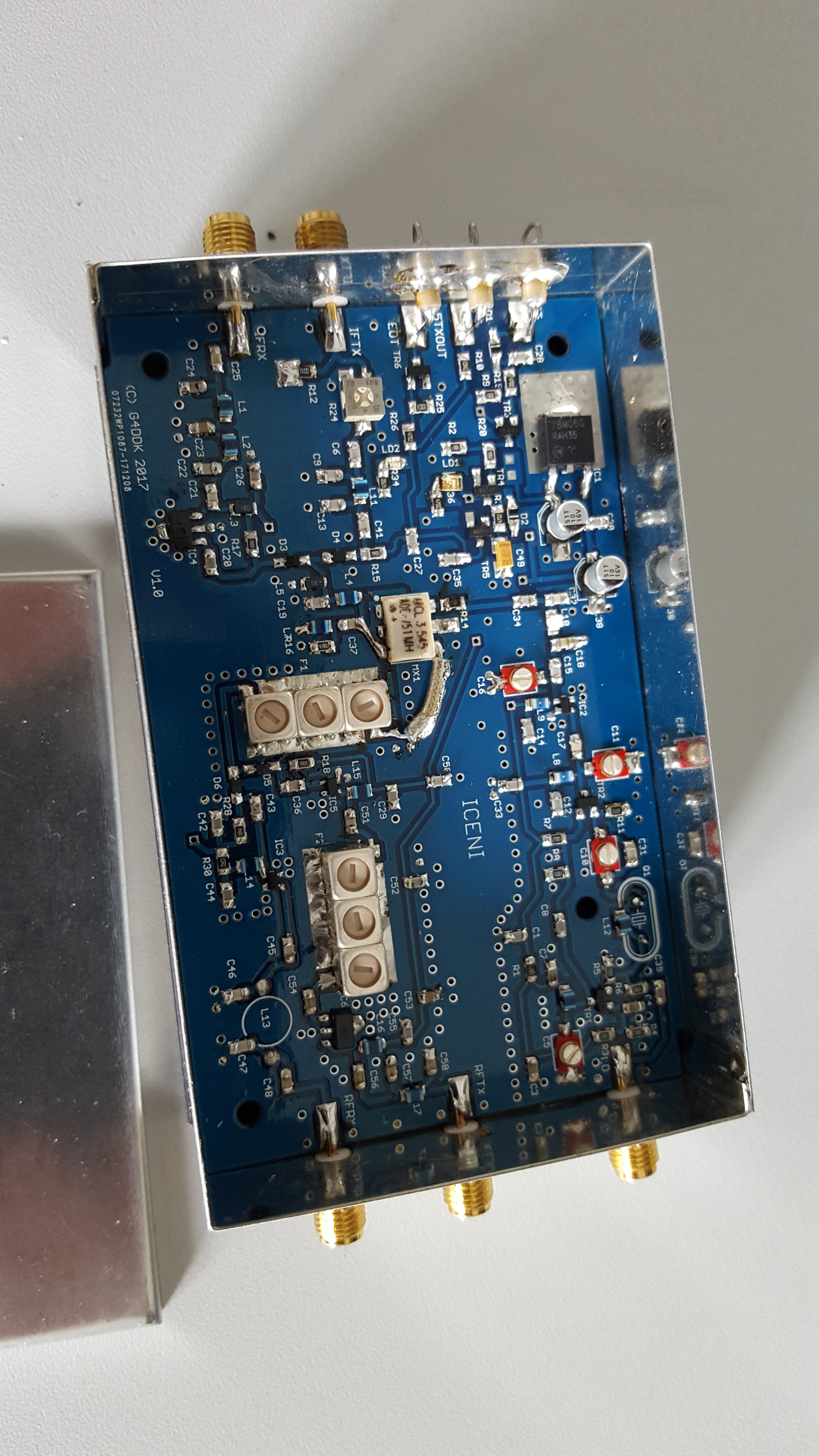
The diagram shows the output power of my G4DDK-Iceni transverter in relation to the input power.
It is quite linear up to 3dBm input / 20dBm output and drops relatively hard above.
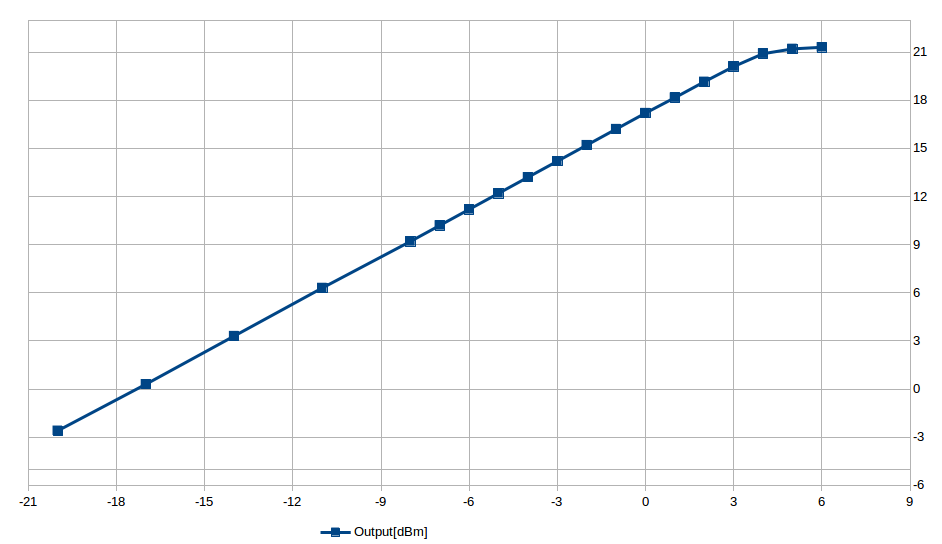
G4DDK Iceni TX gain
The diagram shows the output power of my G4DDK-Iceni transverter in relation to the input power.
It is quite linear up to 3dBm input / 20dBm output and drops relatively hard above.
G4DDK Iceni TX gain
The 1090MHz filters arrived and i measured this variant plus one without filter.
Closer to the filter the response looks quite ok:
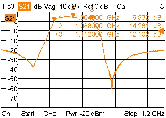
LNA 1090MHz
Far away from the passband the supression degrades. Especially very high frequencies pass the filter quite well.
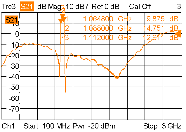
LNA 1090M span 3GHz
This is the assembly with 47pF capacitors and a 27nH coil for supply of the MMIC. Below 200MHz does not pass the capacitors well. There is even some remaining gain at 3.4GHz although its a 1.6mm thick FR4 PCB.

LNA without filter
I have an older OSLO LNB which, was my spare for the websdr. Now i want to use it for QO-100. To improve the temperature stability a TCXO was fitted in place of the original crystal. Find some pictures below.
The type is a TXC 7N-26.000MBP-T from TXC. It works from 2.7 to 5.5V. Luckily the LNB works with 5V from an 7805 regulator. The TCXO was supplied by Michael DG0OPK. He suggested this type and already modified a OTLSO some years ago.
http://www.dg0opk.darc.de/Octagon_LNB_mod_March2017.html
Some warning: This might not apply to current types of the Octagon LNBs. As far as i know you will likely get a 25MHz crystal version if you try to buy one. It will not be possible to use the 25MHz LNB with a lower reference frequency.
LNB with NXP TFF1017 IC could be an alternative as far as i know. I have no experience with this type. Here is some reference:
http://www.pg540.org/wiki/index.php/PLL_LNB
Back to the OSLO:
Modification:
First i removed the crystal. It is necessary to use hot air because otherwise the pads might be damaged. But they are still needed. Also the 0 Ohm resistor over the two traces that go between the two pads needs to be removed. The trace connected to the former crystal pad closer to the RF section needs to be disconnected. This crystal input will be left unconnected.
OSLO LNB with crystal removed
Now a insulated copper wire can be connected to the pad of the former 0 ohm resistor that leads to the converter IC. The capacitor to ground at the crystal pad close to the 7805 regulator needs to be replaced by a short. The other crystal capacitor should be replaced by 100nF.
OSLO prepared for mounting TCXO
Now the TCXO can be soldered. It is important to avoid shorts of the pins of the TCXO towards the PCB. I soldered the TCXO slightly elevated. It is important to keep distance from the border of the PCB because the cap of the LNB still needs to be mounted. The insulated copper wire can be connected to the output of the oscillator which is pin 5 (right of the row of capacitors). The pad with the remaining capacitor towards ground needs to be connected to the output of the 5V regulator. It is the regulator pin with the 0 ohm resistor.
The pins of the TCXO are assigned as: 9=VCC (left of the capacitors), 4=GND, 5=Output.
OSLO with TCXO mounted
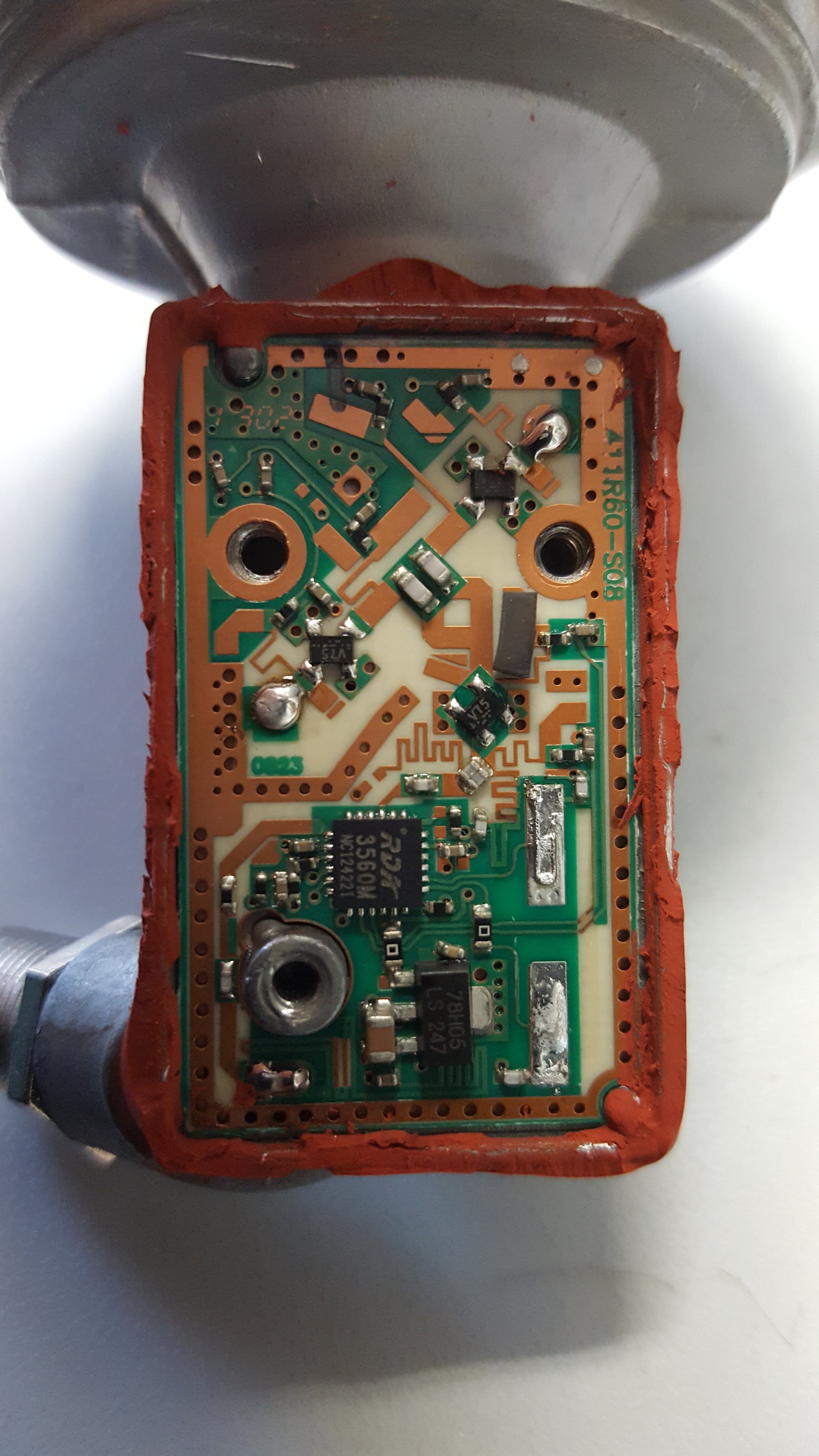
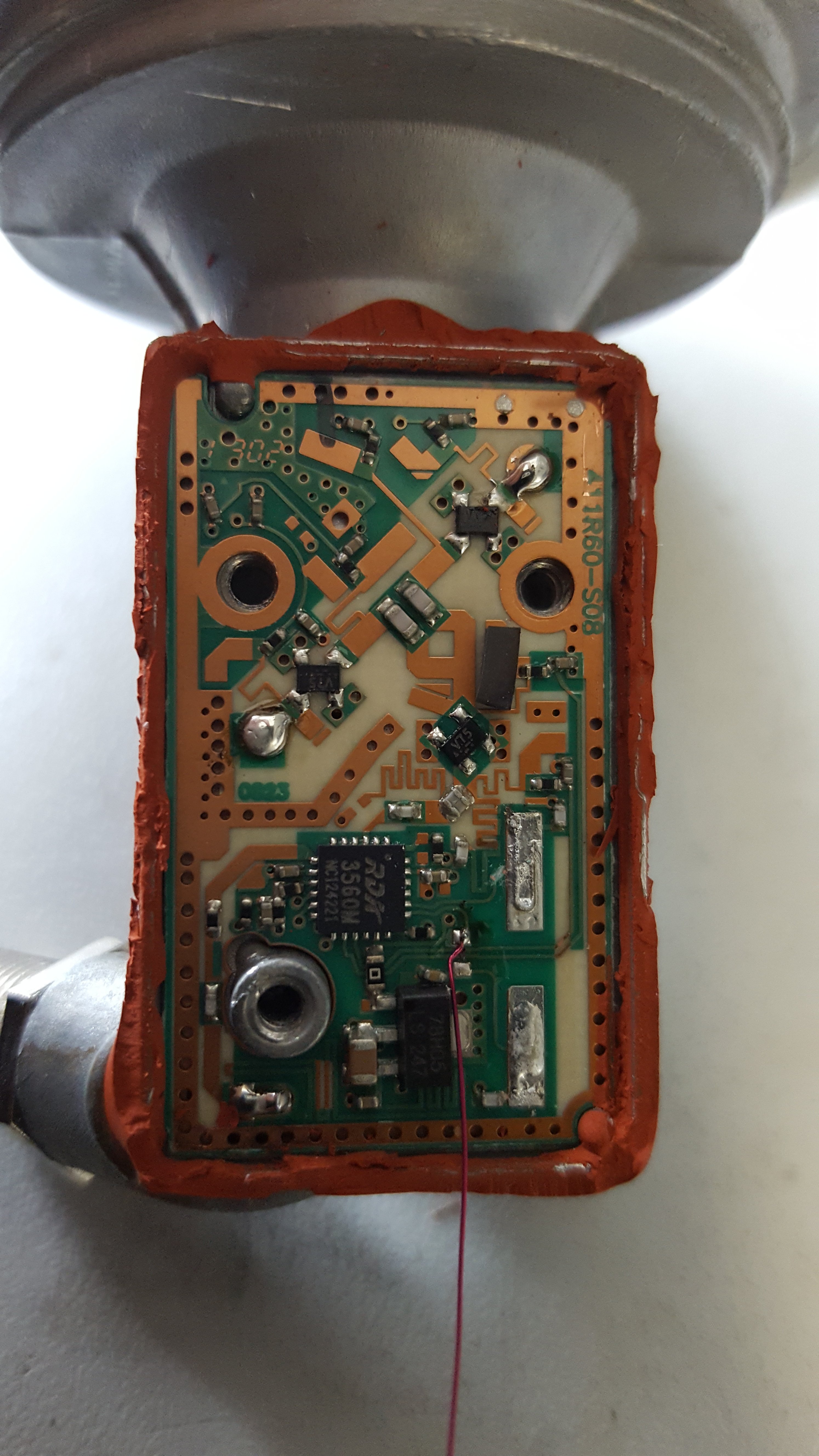
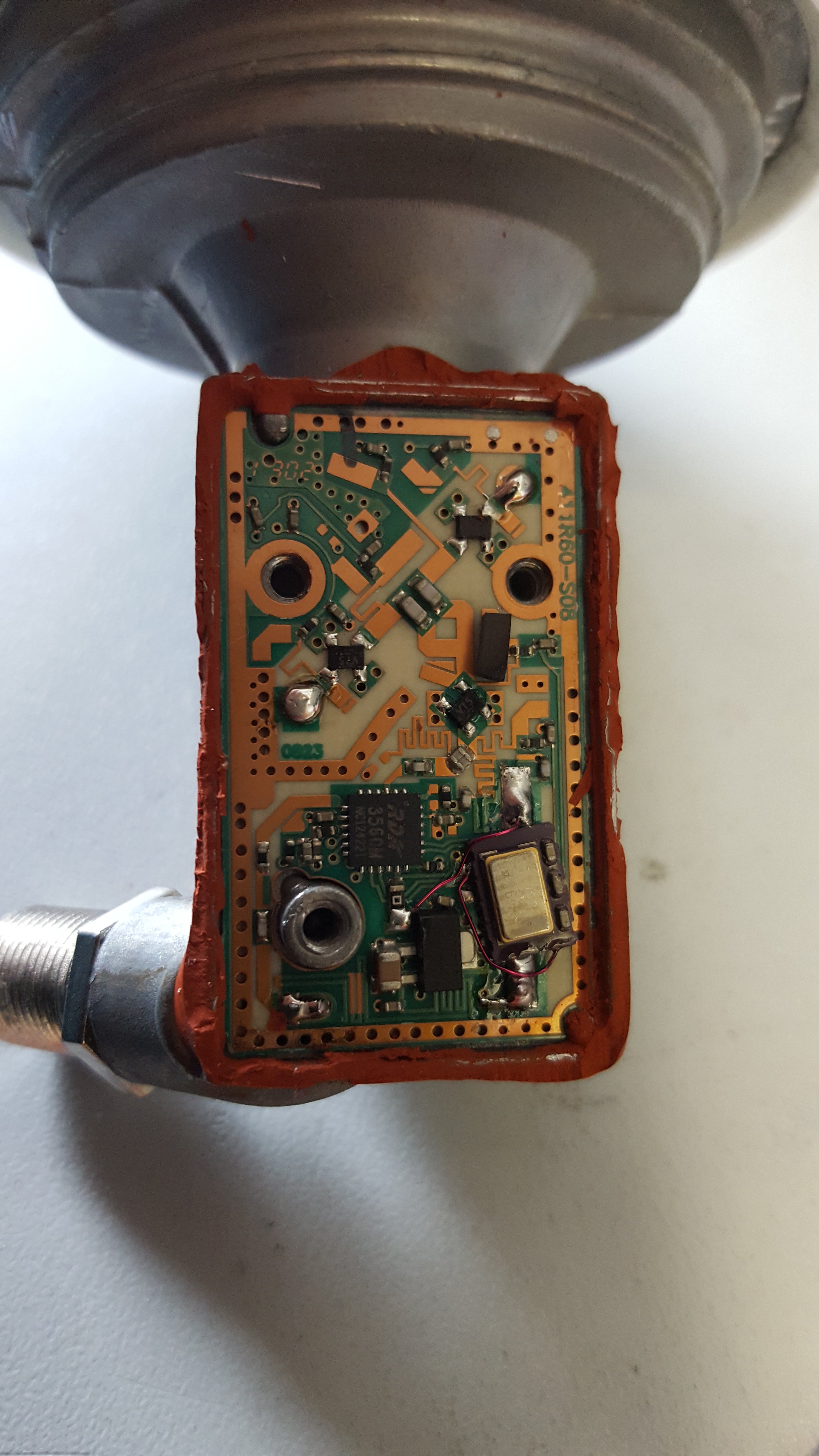
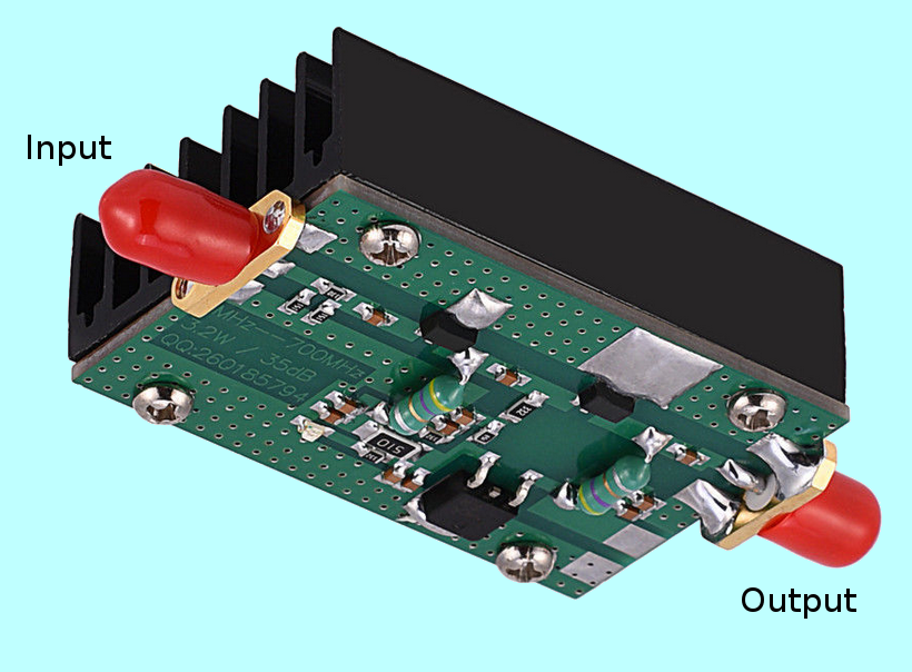
I assembled the Iceni 70cm transverter kit from G4DDK. Instead of the ADE-13 i used a ADE-751MH+. Sam was so kind and sponsored one of his mixer samples he used for testing. Unfortunately the manufacturer of the mixers uses different pinouts for almost every type. In this case i had to swap RF and IP ports. The good one: It is not difficult with the layout. In the picture you can see the short semirigid.
G4DDK Iceni transverter for 70cm
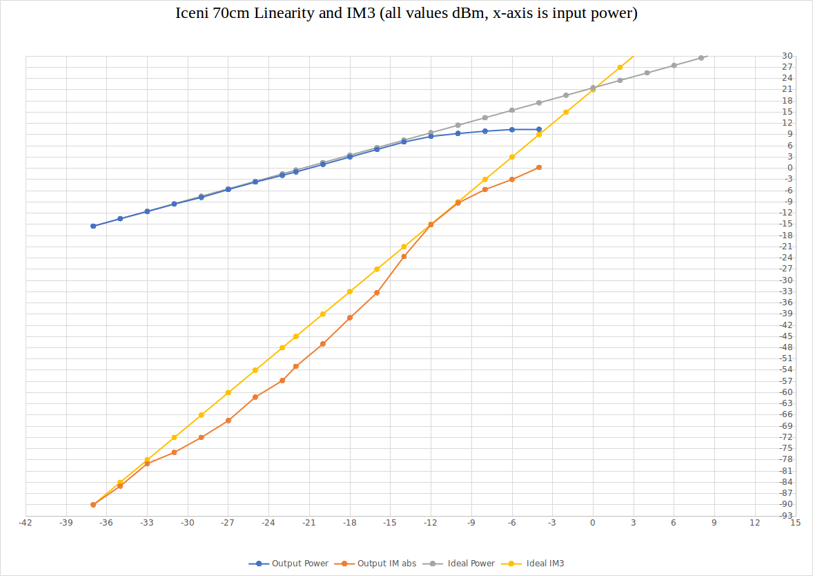
Iceni ADE-751 IM3
I was searching for a small driver for 2m in order to have enough power for my microwave transverters. I usually drive them with about 500mW. Since i have a transverter block with about 0dBm output it needs some gain. Again i found something from China. The advertisement told something about 1.5W, the pictures showed a PCB with a print 35dB/3.2W. However, i thought it could be good enough to get 0.5W out of it.
A small VHF/UHF amplifier
Gain of small VHF/UHF PA
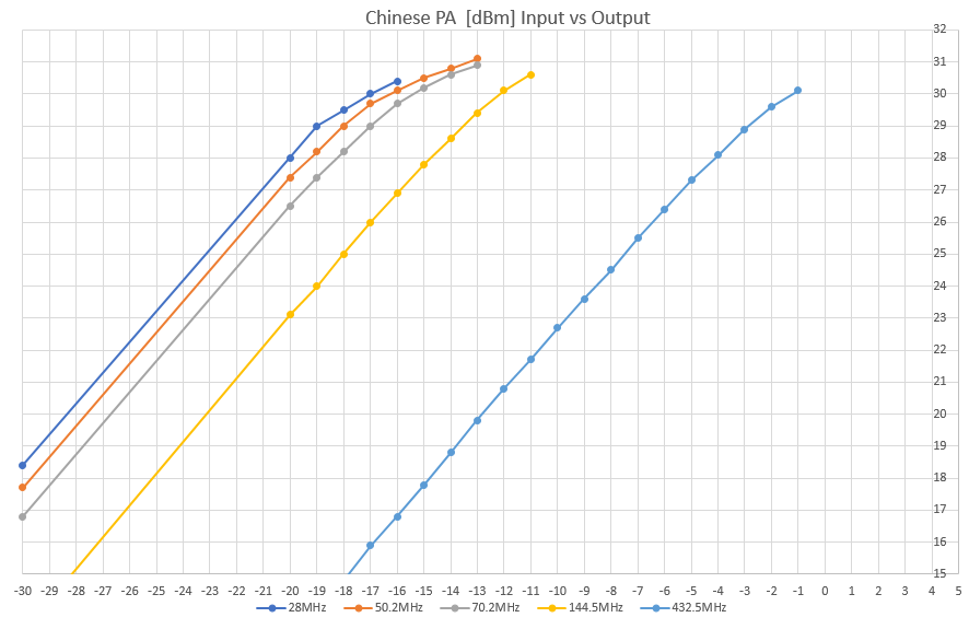
VHF/UHF PA output power
Some posts ago i wrote about my new 6cm transverter. I already did a few QSO and i got a 10W PA for a good price. Unfortunately this PA needs 1W of Input and the transverter gives maximum of 250mW output. So a small “driver” is needed. I was researching the options but found no easy solution that also fits my budget constraints. Then i saw some amplifiers sold as WLAN amp. Usually those are for 2.4GHz but i thought if there are some for the one band there are probably also some for the 5GHz band. During the search i found the nice Amp on the picture below that is sold as an amplifier for video transmissions for about 22Euro. It is specified with 3.5/4.5W. But whatever output power for the price i thought i cannot do wrong a lot.
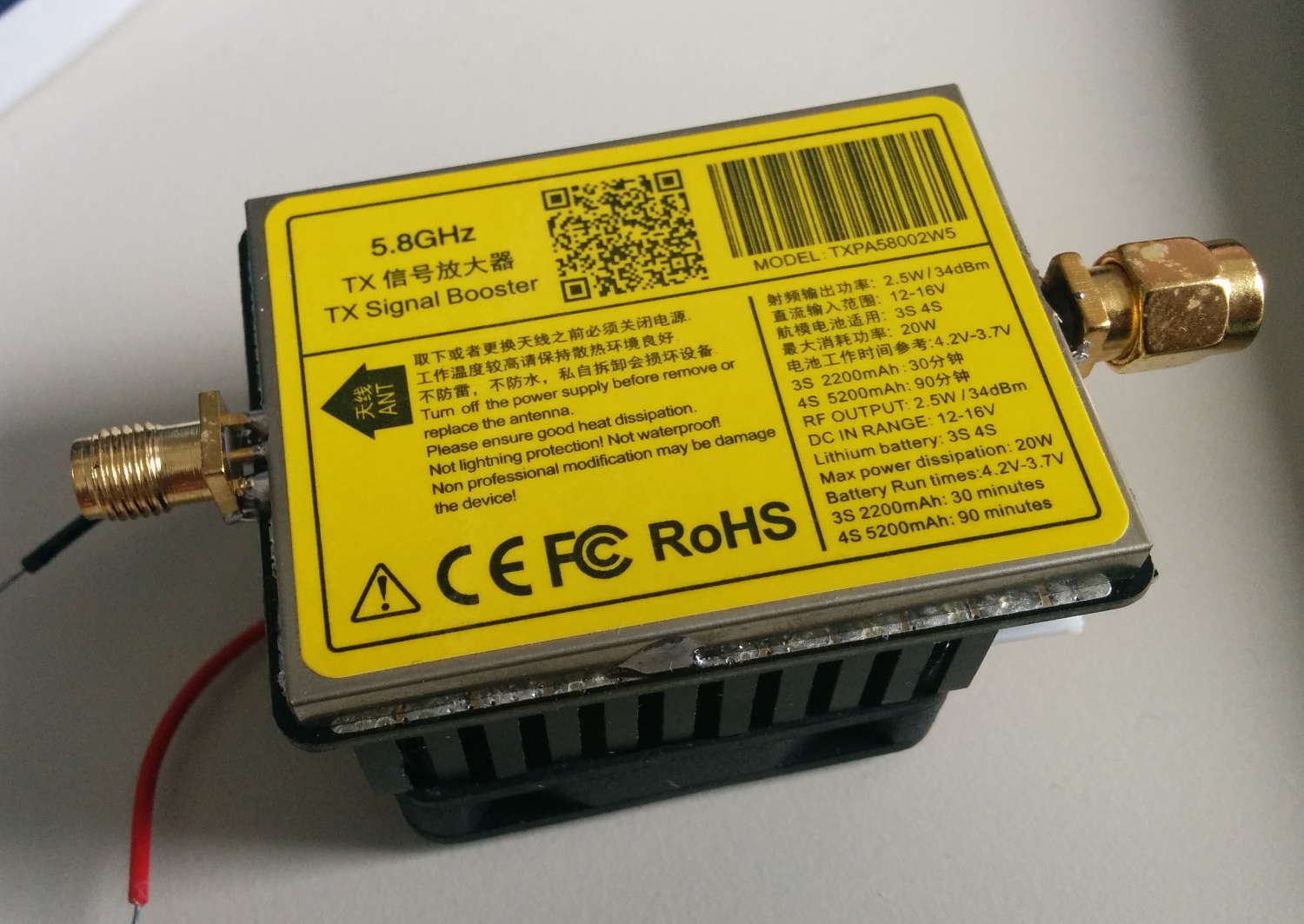
A chinese 5.8GHz PA
When the device arrived i had to find out the supply voltage. In fact it works with 12V and a first test confirmed it has some gain. The bad thing was that the connectors were reverse SMA and for each connector it was quite some gap between the connector and the PCB. So i thought, “thats a strange matching method” ;)
After removing the soldered shield on top of the PCB one of the screws for mounting the heatsink also came out.
The semiconductors used in the PA are 2x Skyworks SE5004L with a P1dB of 30dBm typical and 34dBm max. So i thought 2W should be possible at least. The gain is specified with 32dB. At the input of the PA is a pi-attenuator.
Later i soldered some nice SMA jacks and then the PA went to storage for quite some while.
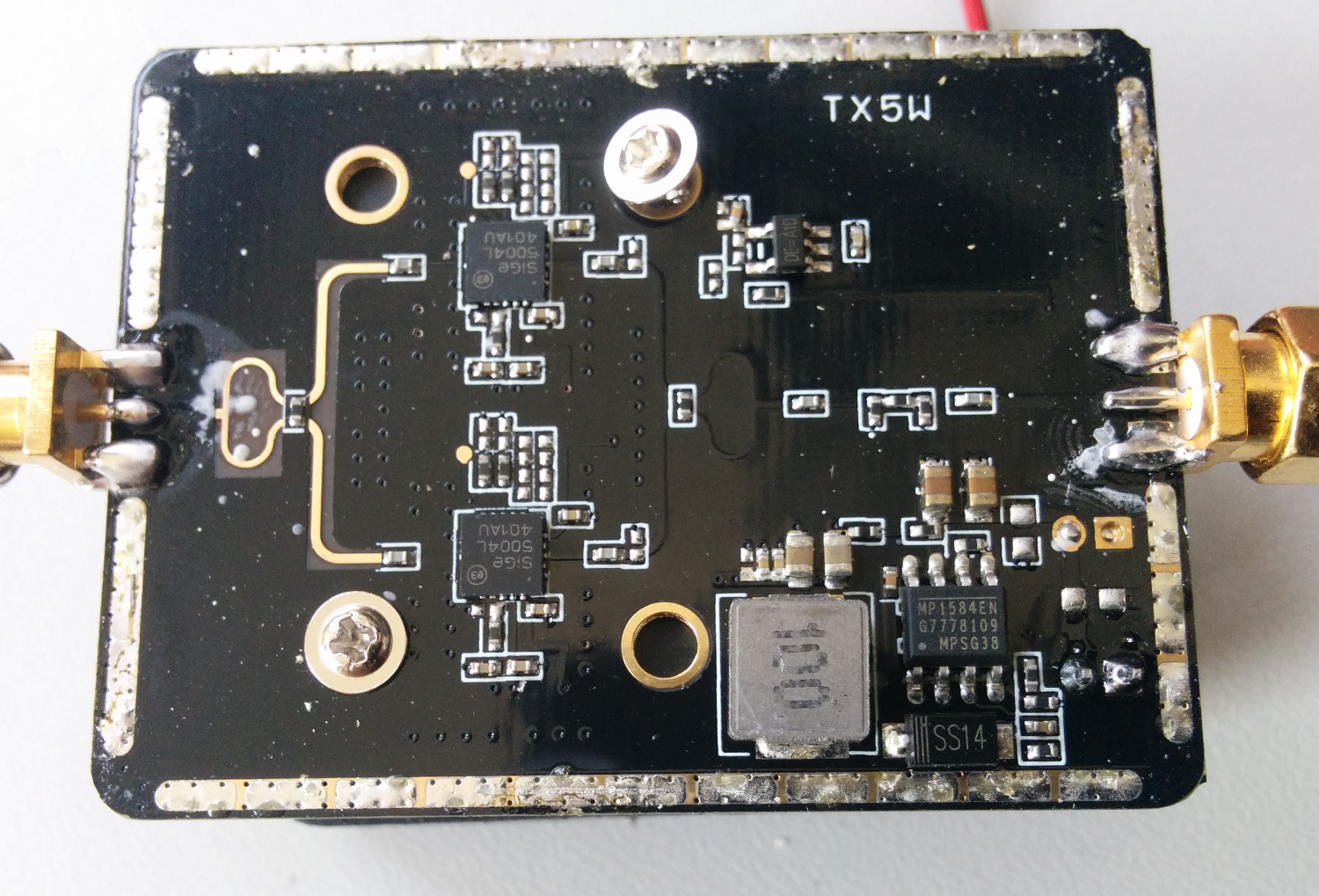
The “inner values” of the small amplifier
Now i found some minutes to remove the attenuator and do some raw measurement of the output power. The gain of the amplifier is about 28..29dB. I did not measure the cable attenuation exactly so do not nail me down on the last dB.
The input vs output figure you can find below. The P1dB is about 2.5W. So considering the samples to be typical there is quite some loss on the PCB. But even in that case for the given price its a nice thing.
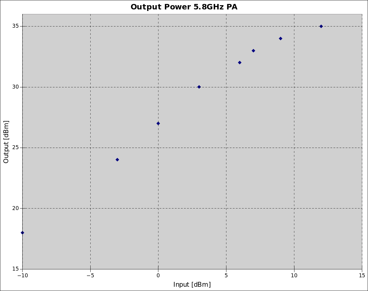
5.8GHz video PA output power
I tested my new assembled wideband high IP amplifier (BX-088) from Funkamateur. The transformers need to be handmade which is a very fiddling task. The cores are really small. I choose for 11dB gain assembly. The measurement shows, that the gain really rapidly drops below the 160m band. The figure fits to what is shown in the documentation. So far i did not measure the p1dB or IM3 behavior.
The points that are interesting for me are 28MHz as LNA for my SDR or as IF amplifier for transverter input on 14/28MHz and usage as pre-amp for 70MHz.
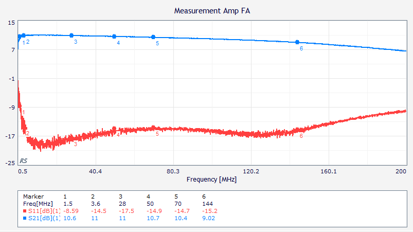
Measurement of Funkamateur wideband amplifier
I was searching for some simple LNA for microwave reception and found a very cheap board from China. For less than 10 Euro i ordered a LNA board that is specified to work from 50MHz to 6GHz. The gain should be about 20dB at 50MHz and still >10dB at 6GHz. Even if it does not work like that the PCB with shield and SMA jacks is still a good deal. You can find some measurement results below. The original condition makes clear that the gain on the upper frequencies is not good. Touching the bias network with the finger showed slight improvements. So it was clear that there is some problem with the components feeding the MMIC. Exchanging the ferrite bead by a 68nH RF coil gives much better results up to 4.5GHz but still has problems on the highest frequencies. So i tried a 2.7nH i series directly connected to the RF trace in order to avoid the stub that was there before. Now 6GHz is good but there is a resonance at about 3.5GHz. My last attempt was an additional 120nF to ground between the two coils. Thats pretty promising for the microwave bands but below 800MHz the LNA is not usable anymore. So the network still has room for improvement but it is at least clear that the board is usable.
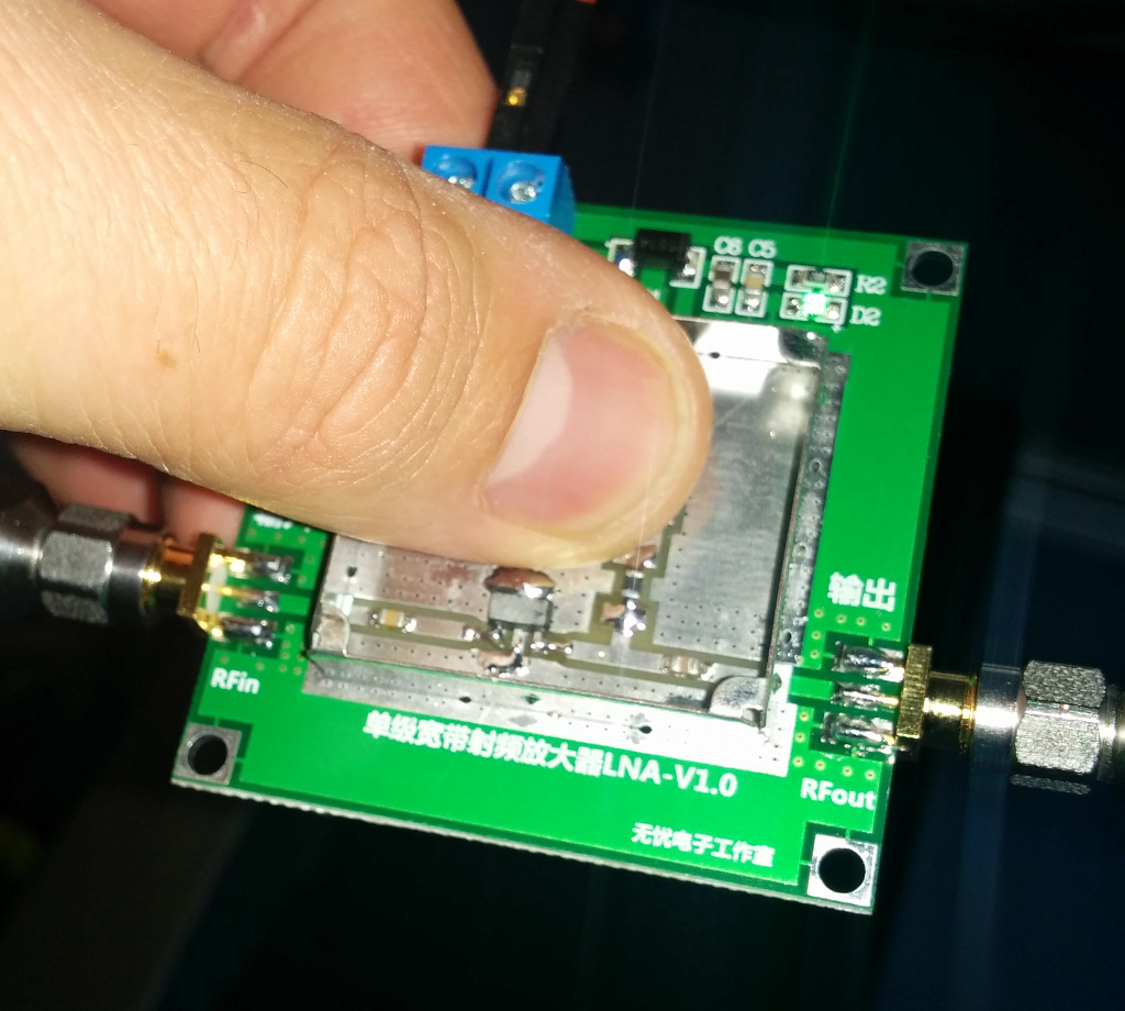
Chinese LNA with german finger ;)
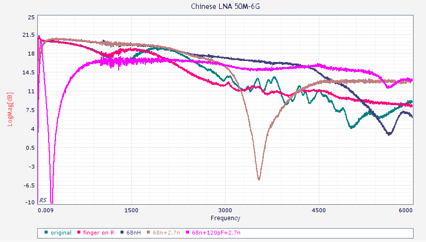
measurement results for different bias networks
Attiny2313 + Uln2003 + highside FET switch for PA + lowside FET switch for RX-TX relais and a few bipolar Low Power stages on a two-layer board. The PTT input can be either high-side or low-side active. It also has lock input to connect several transverter to one antenna system. Via the driver IC a pulse relais and a fan can be controlled. There is also a Tx inhibit output that can be used with Yaesu tranceivers.
Schematic:
Attiny Sequencer Rev2 schematic
The circuit has two PTT inputs and two Error inputs (decoupled by diodes). A active high PTT input is available as well. There is a highside FET switch that can be used to drive a PA and a lowside FET switch that can be used for an RX/TX relais. The TX inhibit signal is available to drive the inhibit input of Yaesu transceivers. The active out is used to signal a sequencer in TX mode. This can be used to lock other sequencers via the error input. The ULN2003 driver is currently configured for another RX/TX relais, a fan which is running until 30s after releasing the PTT, another low active signal parallel to TX-inhibit (as PTT for TRX without TX inhibit) and output signals for a pulse relais (bi-stable RF relais). The serial interface (also used for ISP) is unused in the application. It might be possible to connect a temperature sensor for example.
The missing connection from Q4 to R7 is a print error.
The design was done with KiCad which is a open source PCB layout system. The code for the microcontroller was written in C. The 2k program memory are almost full now but one might be able to optimize. If you are interested in the design data let me know. I also have some spare PCB left over.
I wonder what else could be implemented with this PCB with the small program memory size. Feel free to give some ideas.
something for kids …
AATIS AS001 key