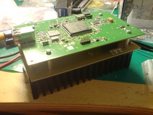
Months ago i heard a talk of Andreas DL5CN about his software defined radio activities. He mentioned a hardware brought up by James N2ADR that works with his Linux SDR software QUISK. In the next both issues of the Funkamateur Guenter DL7LA and Detlef DL7IY described their experiences with the design.
The transceiver is a RF-to-bits design which means that the RF domain is samples with 122MSamples/s and bandfiltered, downconverted within an FPGA and transferred to the PC via an Ethernet interface. The transmit path is the other way around using a D/A converter. The details can be found in their article.
From them i got a commercial 2-layer PCB board with some improvements against the original layout from James. With the information i got from Guenter and Detlef and the info that can be found at James website i started purchasing the parts. It turned out that it is important to notice every piece of information very exact. In addition the power supply for the PCB is not part of the circuit (at least most of it). Therefore much effort needs to be spend to create a proper supply that also takes into account avoiding much noise in the supply for the analog parts of the circuit and avoid too much power dissipation in the regulators.
Last days i completed my power supply which now produces several voltages. 5V digital that supplies the regulators for 3.3V digital 2.5V digital for the FPGA. (An additional 1.2V regulator for the FPGA is located at the transceiver PCB and supplied by the 3.3V). At the analog side there are a 5V regulator for the RX preamp, 3.3V for the A/D, D/A converters and 7.5V for the MMIC TX amplifier. After some debugging i was able to load the FPGA configuration into the configuration flash. Today i was able to receive the first (self generated) signal with the receiver part.
Maximum RF bandwith can be between 25kHz and 500kHz.
There is still much todo. The circuit does still not contain any receiver preselection and no transmit amplifier except the few hundred mW that come out of the MMIC.
A funny thing was that nobody ever showed a picture of the bottom side of the PCB which is more or less a spiders web ;)
You can find further information and some more pictures at the Yahoo group i created for discussions. It can be found at
http://groups.yahoo.com/group/n2adr-sdr/
Rauschfunk
V-U-SHF / SDR / DV and more by Mario, DH5YM

